Spin FV-1 Reverb IC - Featuring Spin Semiconductor Virtual Analog Technology
FEATURES:
General Description
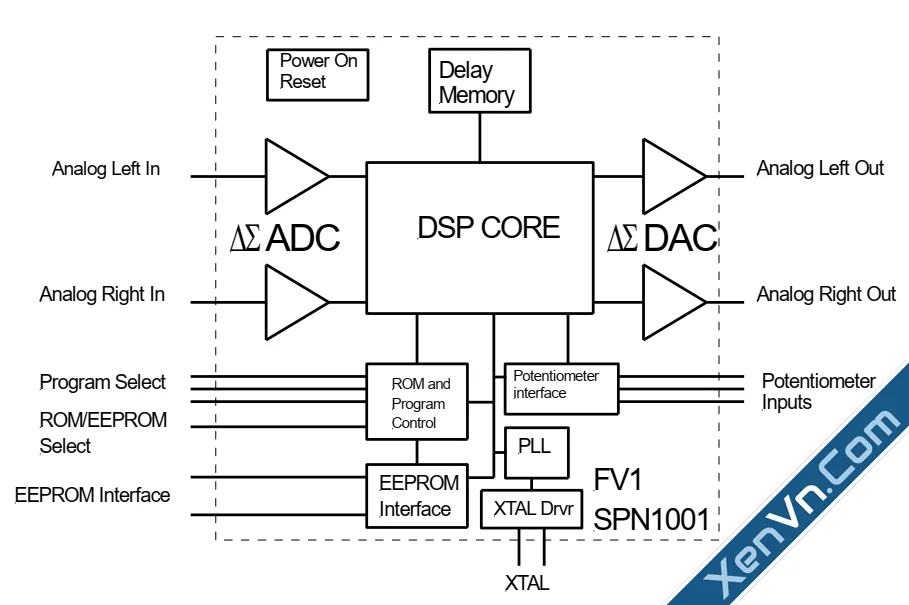
The Spin Semiconductor FV-1 is a complete reverb solution in a single IC. With integrated stereo ADC and DACs, the FV-1 can be treated like any other analog component in your products signal path.
The FV-1 can access a total of 16 programs, 8 programs are built in to the internal ROM and the designer may elect to connect a serial EEPROM with 8 additional programs. By using an external EEPROM, the designer can distinguish his product from others by creating a custom program set without the need for a microprocessor in the system.
With 3 potentiometer inputs, programs may have real time variable parameters such as decay time in a reverb, rate and depth in a chorus or frequency in a filter. These inputs are available as coefficients to your program and may be used independently of each other.
The rich instruction set allows users to program effects of all kinds. With instructions like LOG and EXP, users can easily program audio expansion and compression routines. Integrated digital LFOs and ramp generators allow for programming chorus, flange and pitch shift.
A complete development system including assembler and development board with USB interface are available from Spin Semiconductor. The assembler and instruction set documentation are available free from the Spin web site along with example code that may be freely used in your product.
ROM Programs The FV-1 includes 8 programs in the internal ROM, these programs and the assigned potentiometer input controls are detailed in Table 1.

DSP Core
The DSP core of the FV-1 provides many advanced features and instructions that allow you to create advanced programs to make your product stand out. The DSP core consists of the MAC/ALU where all math and logic instructions take place, the LOG and EXP blocks that perform the log and exponential functions, a 32-register bank separate from the delay RAM
and LFO and ramp generators that can offset memory addressing.
A complete list and description of instructions is available in the assembly language manual that is included on the CD in the development kit or may be downloaded from the Spin Semiconductor web site.
Typical Application
The FV-1 is extremely easy to include in any audio system, but certain details should be considered. For all practical purposes, the FV-1 can be treated as an analog part. Although the FV-1 is fully digital internally, it has been designed with internal power supply bypassing and careful attention to signal pin protection devices so that only a clean power supply
and expected analog techniques are required at the PCB level.
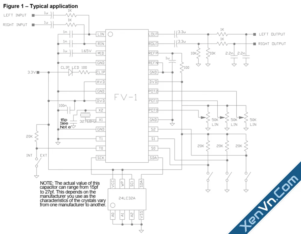
The inputs should be conducted through coupling capacitors, as the inputs are internally biased to a VDD/2 potential. The input signals should be led through 1K resistances with 1nF capacitors directly to ground as close as possible to the input pins. These bypass capacitors should be of good quality, either film capacitors or NP0 (COG) ceramic. The purpose of
this input bypassing is to remove any high frequency noise from the input signals, and to provide a low impedance at very high frequencies.
The outputs may contain out of band noise that can be more fully removed through the use of a two-pole active filter, but for most applications this noise is both inaudible and of no consequence to following circuitry. A simple RC filter is sufficient to remove any high frequency components, if required.
The output mute circuit, internal to the device, inserts a 100K ohm resistance in series with output pins during device power-up, which allows the output coupling capacitors to slowly become biased to the nominal output voltage of VDD/2.
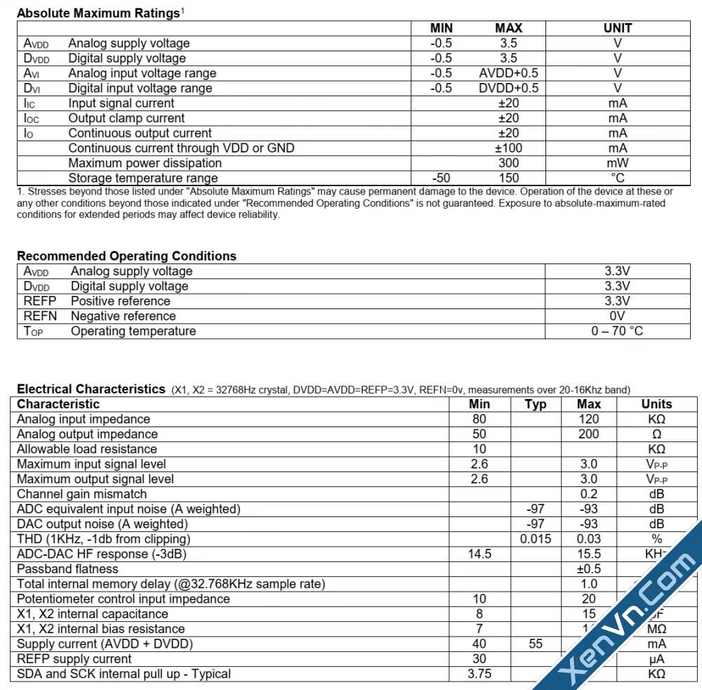
The load resistance on the outputs should be no less than 10K ohms so as to not overload the output drivers, and the coupling capacitor should have a time constant with the load resistance of about 20 to 50ms. The power up delay will be approximately 0.5 to 1 second, depending on crystal properties.
The clip LED is optional, but will flash for approximately 30mS if the internal ADC or the DAC are driven to within a few tenths of a dB of full scale. Any overflow from internal processing that does not produce a near full scale output will not light the clip LED.
Digital power should be bypassed with a ceramic capacitor to ground with very short leads to the part. Ideally, the design will be onto a double sided PCB with the lower layer as a solid pour, connected to ground. This provides a convenient low inductance connection for bypass capacitors through vias. A single sided PCB can be used provided that a large ground
area is included beneath the chip and surface mount bypass capacitors are connected from supply pins to this ground as close to the chip as possible.
Likewise, the REFP and REFN pins should have a bypass cap attached close to the part, with a resistor to supply from VDD. The current drawn by the REFP terminal is small, on the order of 30uA, so there will be only a slight voltage drop across the reference series resistor. The input and output signal levels however, will be a function of the potential across
the REFP and REFN pins. Be careful to not make the series filter resistor between VDD and the REFP pin too large, or signal levels will be affected.
The input resistance of the potentiometer control inputs is on the order of 10 megohms, and these terminals are quite resistant to noise. No bypass capacitors should be required on these terminals. If not required, these terminals may be left open, or if the program includes the use of a potentiometer function, it may be connected to MID if a centered
potentiometer position is desired, but an actual control is not intended in the design.
The crystal oscillator is designed for the standard 32768 Hz watch crystal, as this is particularly inexpensive, but any logic level clock source can be attached to the X1 terminal directly. The sample rate of the system will be at this applied rate. At 32768Hz, the ADC and DAC bandwidth will be 15KHz, at a clock frequency of 48KHz, the bandwidth will expand to
beyond 20KHz. Watch crystals have a very high Q factor, and require significant time to develop full level oscillation. All support components for the crystal are included internal to the device, including a 10Meg bias resistor and two 12pF capacitors. The lead length however, between the crystal and the part must be as short as possible. Further, beware that
the loading of a scope probe on the X1 pin may cause the oscillator to stop. If you wish to check the oscillator's operation, use X2 as a measurement point. Depending on the supplier of the crystal there can be a startup problem with the crystal, it is recommended that all designs include a 15pf capacitor between X2 and ground.
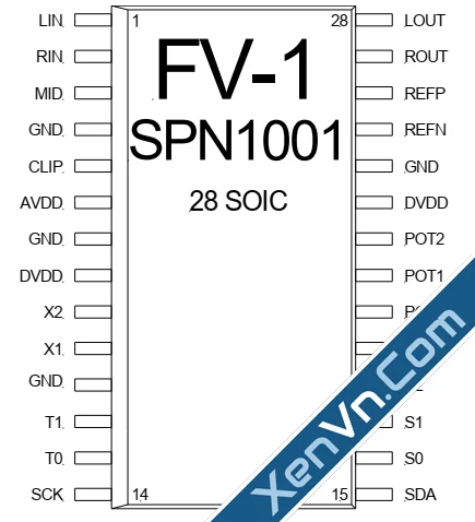
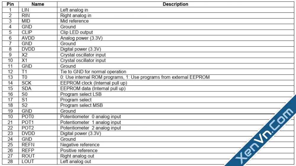
The use of an external EEPROM is optional, and in the case of designs that do not make use of this expansion option, the SCK and SDA pins may be left open. T1 however must be grounded, and T0 must be connected to ground (internal programs) or VDD (EEPROM programs).
Spin Semiconductor reserves the right to make changes to, or to discontinue availability of, any product or service without notice.
Spin Semiconductor assumes no liability for applications assistance or customer product design. Customers are responsible for their products and applications using any Spin Semiconductor product or service. To minimize the risks associated with customer products or applications, customers should provide adequate design and operating safeguards.
Spin Semiconductor make no warranty, expressed or implied, of the fitness of any product or service for any particular application.
FEATURES:
- Integrated stereo ADC and DAC
- 8 internal demonstration programs + 8 external programs
- Easy customization with external EEPROM
- 3 potentiometer inputs for real-time parameter adjustment
- 3.3V operation
- 6 MIPS operation at Fs=48KHz
- 128 instructions/sample clock
- 32K words of delay RAM
- Internal PLL for Fs input clock
- Integrated Power-On-Reset circuit
- LOG and EXP instructions for dynamics
- Green assembly/RoHS compliant
- Guitar Amps
- Mixers
- Effects Equipment
- Karaoke
- Consumer electronics
- Car audio
- Active loudspeaker crossover and flattening
- Industrial processes
General Description
The Spin Semiconductor FV-1 is a complete reverb solution in a single IC. With integrated stereo ADC and DACs, the FV-1 can be treated like any other analog component in your products signal path.
The FV-1 can access a total of 16 programs, 8 programs are built in to the internal ROM and the designer may elect to connect a serial EEPROM with 8 additional programs. By using an external EEPROM, the designer can distinguish his product from others by creating a custom program set without the need for a microprocessor in the system.
With 3 potentiometer inputs, programs may have real time variable parameters such as decay time in a reverb, rate and depth in a chorus or frequency in a filter. These inputs are available as coefficients to your program and may be used independently of each other.
The rich instruction set allows users to program effects of all kinds. With instructions like LOG and EXP, users can easily program audio expansion and compression routines. Integrated digital LFOs and ramp generators allow for programming chorus, flange and pitch shift.
A complete development system including assembler and development board with USB interface are available from Spin Semiconductor. The assembler and instruction set documentation are available free from the Spin web site along with example code that may be freely used in your product.
ROM Programs The FV-1 includes 8 programs in the internal ROM, these programs and the assigned potentiometer input controls are detailed in Table 1.
DSP Core
The DSP core of the FV-1 provides many advanced features and instructions that allow you to create advanced programs to make your product stand out. The DSP core consists of the MAC/ALU where all math and logic instructions take place, the LOG and EXP blocks that perform the log and exponential functions, a 32-register bank separate from the delay RAM
and LFO and ramp generators that can offset memory addressing.
A complete list and description of instructions is available in the assembly language manual that is included on the CD in the development kit or may be downloaded from the Spin Semiconductor web site.
Typical Application
The FV-1 is extremely easy to include in any audio system, but certain details should be considered. For all practical purposes, the FV-1 can be treated as an analog part. Although the FV-1 is fully digital internally, it has been designed with internal power supply bypassing and careful attention to signal pin protection devices so that only a clean power supply
and expected analog techniques are required at the PCB level.
The inputs should be conducted through coupling capacitors, as the inputs are internally biased to a VDD/2 potential. The input signals should be led through 1K resistances with 1nF capacitors directly to ground as close as possible to the input pins. These bypass capacitors should be of good quality, either film capacitors or NP0 (COG) ceramic. The purpose of
this input bypassing is to remove any high frequency noise from the input signals, and to provide a low impedance at very high frequencies.
The outputs may contain out of band noise that can be more fully removed through the use of a two-pole active filter, but for most applications this noise is both inaudible and of no consequence to following circuitry. A simple RC filter is sufficient to remove any high frequency components, if required.
The output mute circuit, internal to the device, inserts a 100K ohm resistance in series with output pins during device power-up, which allows the output coupling capacitors to slowly become biased to the nominal output voltage of VDD/2.
The load resistance on the outputs should be no less than 10K ohms so as to not overload the output drivers, and the coupling capacitor should have a time constant with the load resistance of about 20 to 50ms. The power up delay will be approximately 0.5 to 1 second, depending on crystal properties.
The clip LED is optional, but will flash for approximately 30mS if the internal ADC or the DAC are driven to within a few tenths of a dB of full scale. Any overflow from internal processing that does not produce a near full scale output will not light the clip LED.
Digital power should be bypassed with a ceramic capacitor to ground with very short leads to the part. Ideally, the design will be onto a double sided PCB with the lower layer as a solid pour, connected to ground. This provides a convenient low inductance connection for bypass capacitors through vias. A single sided PCB can be used provided that a large ground
area is included beneath the chip and surface mount bypass capacitors are connected from supply pins to this ground as close to the chip as possible.
Likewise, the REFP and REFN pins should have a bypass cap attached close to the part, with a resistor to supply from VDD. The current drawn by the REFP terminal is small, on the order of 30uA, so there will be only a slight voltage drop across the reference series resistor. The input and output signal levels however, will be a function of the potential across
the REFP and REFN pins. Be careful to not make the series filter resistor between VDD and the REFP pin too large, or signal levels will be affected.
The input resistance of the potentiometer control inputs is on the order of 10 megohms, and these terminals are quite resistant to noise. No bypass capacitors should be required on these terminals. If not required, these terminals may be left open, or if the program includes the use of a potentiometer function, it may be connected to MID if a centered
potentiometer position is desired, but an actual control is not intended in the design.
The crystal oscillator is designed for the standard 32768 Hz watch crystal, as this is particularly inexpensive, but any logic level clock source can be attached to the X1 terminal directly. The sample rate of the system will be at this applied rate. At 32768Hz, the ADC and DAC bandwidth will be 15KHz, at a clock frequency of 48KHz, the bandwidth will expand to
beyond 20KHz. Watch crystals have a very high Q factor, and require significant time to develop full level oscillation. All support components for the crystal are included internal to the device, including a 10Meg bias resistor and two 12pF capacitors. The lead length however, between the crystal and the part must be as short as possible. Further, beware that
the loading of a scope probe on the X1 pin may cause the oscillator to stop. If you wish to check the oscillator's operation, use X2 as a measurement point. Depending on the supplier of the crystal there can be a startup problem with the crystal, it is recommended that all designs include a 15pf capacitor between X2 and ground.
The use of an external EEPROM is optional, and in the case of designs that do not make use of this expansion option, the SCK and SDA pins may be left open. T1 however must be grounded, and T0 must be connected to ground (internal programs) or VDD (EEPROM programs).
Spin Semiconductor reserves the right to make changes to, or to discontinue availability of, any product or service without notice.
Spin Semiconductor assumes no liability for applications assistance or customer product design. Customers are responsible for their products and applications using any Spin Semiconductor product or service. To minimize the risks associated with customer products or applications, customers should provide adequate design and operating safeguards.
Spin Semiconductor make no warranty, expressed or implied, of the fitness of any product or service for any particular application.